Flip Flop Block Diagram - SR, JK, D, T, Master Slave
Flip Flops are sequential logic circuits that can store information. Flip flops are the basic fundamental circuits of computers and other digital electronic devices. A flip-flop may have one or more inputs and one or more outputs. It is a very basic storage element in digital electronics. Most of the gated flip flop requires a clock pulse to change their operation state. A flip-flop may be level-triggered or edge-triggered. Flip-flop stores data in binary form and it can store a single bit of data that has two states. One state represents 'High' or '1' while another one represents 'Low' or '0'.
There are mainly four types of Flip Flops which are mostly used for practical electronic circuits. Two same flip flops can be connected to use as master-slave flip flops. Anyway in this article, we are going to see the block diagram of all types of flip flops.
SR Flip Flop Block Diagram
Here you can see the block diagram of SR Flip Flop without a gate trigger or enable terminal. So, here we cannot change the state of the operation.
You can see, it has main two input terminals named as 'S' and 'R'. It also has two output terminals named as Q and Q'. You can see there is no additional enable terminal.
Now, here you can see the block diagram of SR Flip Flop with Gate Triggered or Enable Terminal.
From the above two block diagrams, you may notice, in the non-gated SR flip flop, both the 'S' and 'R' input terminals are Active Low terminals but in the case of the gated SR flip, both the S and R input are the active high terminals.
JK Flip Flop Block Diagram
Here, you can see the block diagram of JK Flip Flop. It has two data inputs J and K and two data outputs Q and Q'. It has an additional input terminal for Enable.
Here, J is the SET and K is the RESET. When both the J and K terminals are kept at a high level, the flip flop will get the flip or toggle command. When J=0 and K=1, the flip flop will get the SET command, and when J=1 and K=0, the flip flop will get the RESET command.
D Flip Flop Block Diagram
Here, you can see the block diagram of D Flip Flop. It has only one data input 'D' and two outputs - non-inverted output Q and Inverted Output Q'.
The D flip flop is also known as Data Flip Flop or Delay Flip Flop. Basically, it takes the input from the data input terminal at a definite portion of a clock cycle and the input data goes to the Q output. At other times the output Q does not change.
T Flip Flop Block Diagram
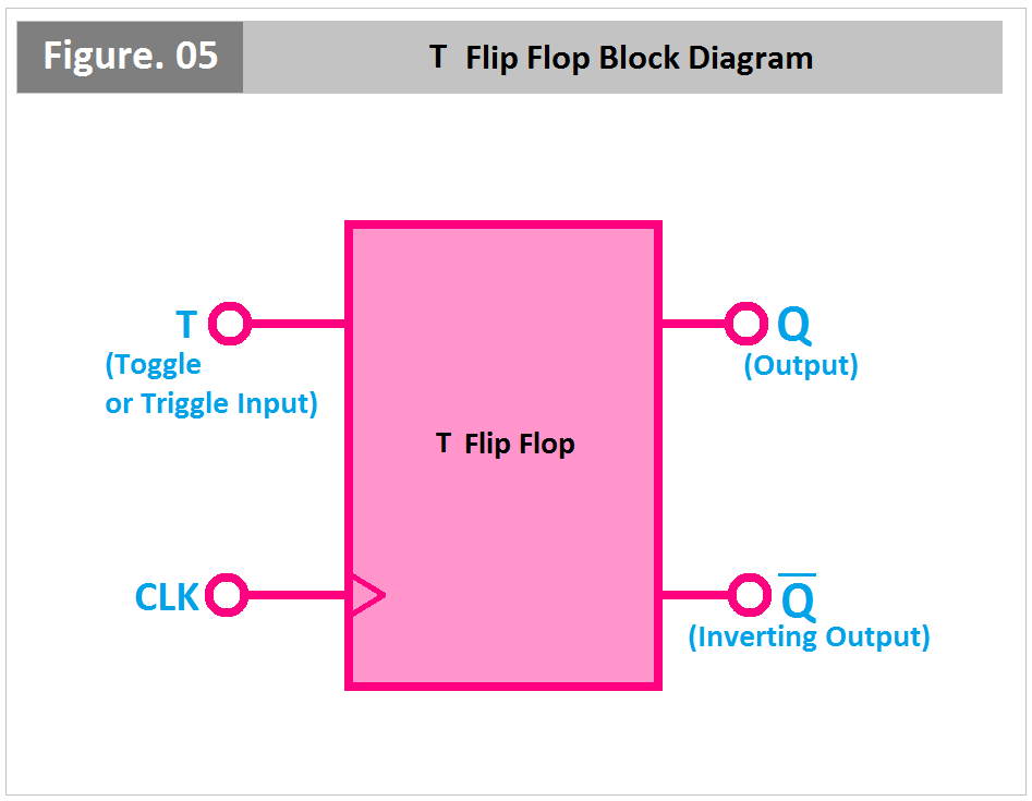
Here, you can see the block diagram of T Flip Flop. It also has a single data input terminal T. It is called Toggle Input or Triggle Input. It has two output terminals including inverting and non-inverting. It has an additional terminal for enabling at the input side.
Basically, when the T input is high the T flip flop changes its state and when the T input is low it holds the previous value.
Master Slave Flip Flop Block Diagram
Here, you can see the block diagram of Master Slave JK Flip Flop. Master-slave flip flops are not only built with JK flip flops but they can be built with other flip flops also. Two same or different flip flops are to be connected one after another.
Here, the first JK flip flop is considered as Master, and the second JK flip flop is considered as Slave. The inputs of the second one are connected to the output of the first one. Clock terminals of both flip flops are connected through a Not gate. So when the first one is in the high state the second one will be in the low state and vice-versa.
Read Also:
- Half Adder and Full Adder Circuit Diagram, Truth Table
- Truth Table and applications of all types of Flip Flops-SR, JK, D, T, Master-Slave
- [Actual] Difference Between Latch and Flip Flop Explained
- Difference Between Combinational and Sequential Circuit
- [BEST] Application and Uses of Logic Gates with Practical Examples

.png)
.png)


.png)