Field Effect Transistor(FET) Symbol, Diagram, Applications
Field Effect Transistor or FET is a huge usable transistor in electronics applications. FET is a transistor that uses the electric field to control the electrical current flow through it that is why it is called a Field Effect Transistor. FET is also known as a unipolar transistor as it uses a single charge carrier for its operation. For example, either it uses electrons or holes as charge carriers but not both at the same time like a Bipolar Junction Transistor(NPN or PNP). It is a voltage-controlled device. The applied voltage to its gate terminal can control the size of the conductive channel so the flow of current through it also changes. The core characteristic of a FET is a very high input impedance at low frequency.
A field-effect transistor has main three common terminals named as - 1. Source(S) 2. Gate(G) and 3. Drain(D). The source is the terminal through which the charge carrier enters into the channel. Generally, this terminal is identified as the English letter S, and the source is denoted by Is. The drain is the terminal through which the charge carrier leaves the channel. Generally, the drain terminal is denoted by the English letter D and the drain current is denoted by ID. On the other hand, the Gate terminal is one where voltage is applied to adjust or modulate the channel conductivity so the drain current can be controlled.
Field Effect Transistor(FET) Symbol
As we know there are so many types of FET so each of them has different symbols. Here you can see the symbols,
Junction Field Effect Transistor(JFET) - P Channel
Junction Field Effect transistor or JFET is a very simple type of FET than others. There are two types of JFET - N Channel and P Channel. In the case of the P channel JFET when the voltage to the gate with respect to the source terminal is positive and gradually increasing the current conduction will be decrease. If we apply a negative voltage then the current flow will not be controlled.
Here, you can see the symbol of JFET below,
N Channel JFET
For N channel JFET we have to apply a negative voltage to its gate terminal with respect to the source terminal to control the current flow through it. So remember that when the gate voltage is zero for the JFET it will conduct current with full capacity. The conductivity will decrease or resistivity will increase when we apply a voltage to its gate terminal.
Here, you can see the symbol of N Channel JFET,
P Channel enhancement Type MOSFET
MOSFET means Metal Oxide Semiconductor Field Effect Transistor. In MOSFET Silicon dioxide is used to form the gate of the MOSFET that provides insulation between the gate and conductive channel to prevent the direct flow of charges. The operation of the enhancement type MOSFET is opposite to the JFET. Here we have to apply the voltage to the gate to turn on the transistor. For P channel MOSFET we have to apply positive voltage.
Here, you can see the symbol of P Channel MOSFET.
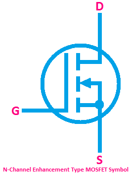
N Channel MOSFET (enhancement Type)
N channel MOSFET required a negative voltage to start its operation. Here you can see the symbolic difference between the N channel and the P channel. For the N channel, the arrow mark is towards to the gate terminal whereas in the P channel, the arrow mark is backward to the gate terminal.
Here, you can see the symbol of N Channel MOSFET.
Depletion Type MOSFET(P-Type)
Depletion Type MOSFET Symbol(N Channel)
The operation of the depletion type MOSFET is opposite to the enhancement type MOSFET and the same as the JFET. In normal conditions, when there is no voltage the depletion type MOSFET will conduct current to control the current flow, or to reduce we have to apply a voltage.
FET Applications
1. As we know the FET is a voltage-controlled device so it is best to build the voltage amplifiers.
2. MOSFET is capable of working with high power so you will see its applications in power electronic circuits such as inverter circuits, power control circuits, etc.
3. In integrated circuits, analog circuits, and digital circuits you can see the applications of Field Effect Transistors.
Read Also:
- Difference between NMOS, PMOS, CMOS Transistor with Symbols
- What is Common Emitter Configuration in Transistor Amplifier?
- UJT Application, Uses, Advantages, Diagram, Symbol, Circuit
- [Actual] Difference between Analog and Digital Signal with Examples
- [BEST] Applications and Uses of Tunnel Diode with Advantages


