Transistor Diagram, Parts and Terminals
Here in this article, we are going to see the Transistor Diagram and learn about its different parts and terminals. The transistor is an electronic semiconductor device that acts as an amplifier or an electronic switch. It is the most important and useful electronic component of electronics engineering. Almost all electronic devices use transistors, in fact without a transistor digital circuit can not be built.
A typical transistor is a three-layer device and has a minimum of three terminals to connect it to an external electrical or electronic circuit. A transistor can work as both an amplifier and a switch in analog circuits and works as a switch in digital circuits. The transistor was introduced in 1947 and changed the world of technology and engineering.
Transistor Parts
There are different types of transistors available according to their construction, characteristics, and working principles. Here, we will talk about BJT or Bipolar Junction Transistors. The term bolar implies that here both carriers mean electrons and holes are responsible for the current conduction. It is the most common low-power transistor.
On the other hand, in a unijunction transistor, anyone either a hole or electron is responsible for the current conduction. There are two types of Bipolar Junction Transistors - PNP transistors and NPN transistors. The basic three parts of these both types of transistors are,
- Semiconductor Layers(P-type layer or N-type Layer)
- Junction
- Terminals
The PNP transistor is made of two P-type layers and one N-type layer whereas the NPN Transistor is made of two N-type layers and one P-type layer.
The junction in a transistor is the barrier that initially resists the flow of electric current. By applying a voltage across it and varying the applied the flow of current can be controlled.
The terminals help to connect all the layers of the transistor to the external circuit.
Transistor Terminals
There are mainly three terminals of a Bipolar Junction Transistor,
- Collector
- Base
- Emitter
The collector is the positive lead of the transistor whereas the emitter is the negative lead of the transistor and the base is common, generally it is connected to the ground.
Filed effect transistor has three terminals named as,
- Source
- Gate
- Drain
Read Also:
Transistor Diagram
Here, you can see the diagram of the NPN Transistor,
Figure (1) shows the actual physical diagram and terminals of the NPN transistor. If you hold the transistor flat side toward your face then the left side terminal is the collector, the middle terminal is the base and the right side terminal is the emitter. The figure (2) shows the symbolic diagram of the NPN Transistor. And the figure (3) shows the construction diagram. Here, you can see, it has two n-type layers and one p-type layer. Also, you can see it has three layers and two junctions. Both n-type layers are connected to the collector and emitter whereas the p-type layer is connected to the base.
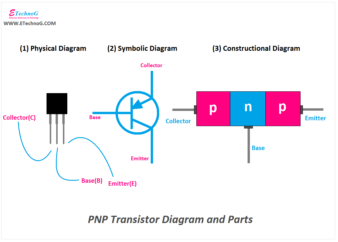
Here, you can see the diagram of the PNP Transistor,
You can see in the PNP transistor, there are two p-type layers and one n-type layer. The p-type layers are connected to the collector and emitter whereas the n-type layer is connected to the base.
Read Also:
Transistor Diagram, Parts and Terminals
 Reviewed by Author
on
November 11, 2021
Rating:
 Reviewed by Author
on
November 11, 2021
Rating:


