Microcontroller 8051 Pinout Diagram and Pin Description
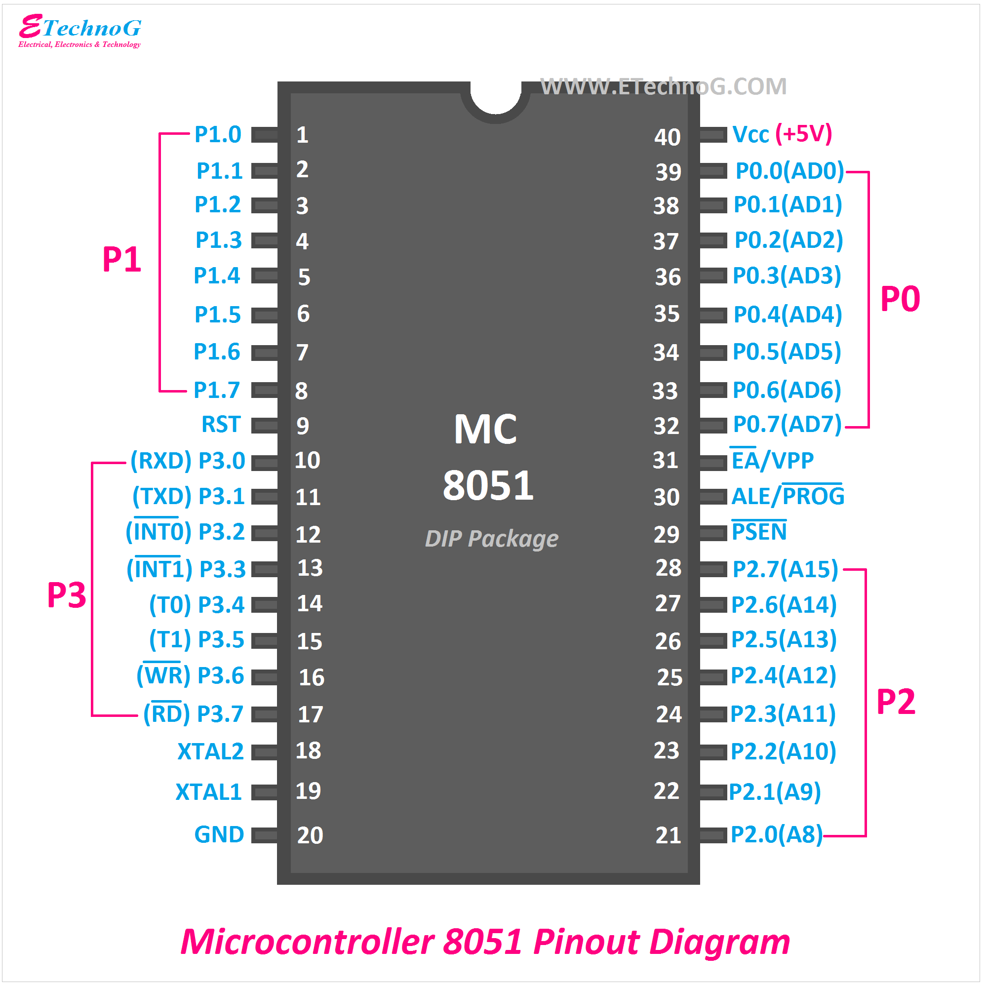
The microcontroller is a Dual Inline Package(DIP) integrated circuit and to has a total of 40 pins. It has a total of four input/output ports and each port has 8 pins. So among the 40 pins, for ports cover the total of 32 pins other pins are used for other functions such as interrupt, power supply, oscillation, etc.
Here, you can see the pin diagram of microcontroller 8051
Pin 1 to 8
The pins from 1 to 8 are named as P1.0, P1.1, P1.2, P1.3, P1.4, P1.5, P1.6, P1.6, P1.7. These are the pins of Port 1. These are bidirectional pins which means data can flow in both directions through these pins. These pins are used for input and output operations. Using the logic control system, it is ensured that those pins will act as input or output. For example, if the logic is high or 1, these pins will act as input pins, but if the logic is low or 0, these pins will act as output pins. The number just after the P indicates the port number. In this case, P1 means port 1. The number after the point indicates the numbering of each pin of that particular port. For example, P1.0 indicates the first pin of port 1 and P1.7 indicates the 7th pin of port 1.
Pin No. 9
Pin 9 of the 8051 microcontrollers is RST or RESET. It is used to reset the microcontroller. It is the active high pin. When reset is done through this pin, the microcontroller terminates its all operations and comes to its initial value. After just turning on the microcontroller, it makes reset, that is why it is also called "Power-ON-Reset".
Pin 10 to 17
Pins 10 to 17 are the pins of the port whose first pin is P3.0 and the last pin is P3.7. These pins are also bidirectional and used for input/output functions. These pins are also used for other functions such as,
- Pin no 10 or P3.0(RXD) - it is the serial input pin that is used to receive serial data
- Pin no 11 or P3.1(TXD) - it is the serial output pin that is used to transmit the serial data
- Pin no 12 and 13 or P3.2 and P3.3 - These are the external hardware interrupt pins(INT0' and INT1'). Using these external interrupts can be raised, so the microprocessor stops its own work and start the work given by the interrupt
- Pin no 14 and 15 or P3.4 and P3.5 - T0, T1 pins are for timer 0 and timer 1 respectively and they can be used to connect external 16-bit timer or counter
- Pin no 16 and 17 or P3.5 and P3.6 - These are the write(WR') and read(RD') terminals. These pins are used to store data in external memory or fetch data from the external memory.
Pin no 18 and 19
Pin no 18 is XTAL2 and 19 is the XTAL1. These pins are used to connect an external crystal oscillator. These pins can handle clock frequencies from 4MHz to 30MHz. The microcontroller receives the clock signal from the crystal oscillator through these pins.
Pin no 20
Pin no 20 is the ground pin, it is used to connect the negative terminal of the power source.
Pin no 21 to 28
These are the pins of port 2 whose P2.0 is the first pin and P2.7 is the last pin. These are the bidirectional pins and used to carry the address bytes.
Pin no 29
Pin no 29 is the PSEN which means Program Store Enable. It is an active low pin. that is mainly used when the microcontroller reads an external memory.
Pin no 30
Pin no 30 acts as both ALE(Address Latch Enable) and PROG(Program Pulse Input). It acts as ALE and makes distinguish between multiple memory chips connected to the microcontroller. It acts as a PROG during flash programming.
Pin no 31
It acts as EA/VPP. EA means External access. It is used to start and stop the interfacing between the external memory chip and the microcontroller.
Pin no 32 to 39
These are the pins of port 0. The P0.0 is the first pin and P0.7 is the last pin. These are the input/output bidirectional pins and used to carry both address and data bytes.
Pin no 40
Pin no 40 is the Vcc. It is used to connect the positive terminal of the power source.
Read Also:
Microcontroller 8051 Pinout Diagram and Pin Description
 Reviewed by Author
on
November 23, 2021
Rating:
 Reviewed by Author
on
November 23, 2021
Rating:

