Phototransistor Symbol, Construction, Circuit, Connection
The phototransistor is an electronic semiconductor device that can sense light and allow the flow of current through it. The phototransistor is an electronic switching and current amplifying device. The current amplifying property of the phototransistor differs from the photodiode because the photodiode also works almost the same but it can not amplify current.
There are two types of phototransistors, BJT phototransistors, and FET phototransistors. Phototransistor works on the same principle as the normal transistor. Just the difference is, in a normal transistor, we need to apply a voltage to the base terminal to activate but in the phototransistor, no voltage needs to apply its base. When light falls upon its base it got activated and starts to conduct current.
Phototransistor Symbol
Here, you can see the symbol of phototransistor below.
You can see the symbol of phototransistor is almost the same as the normal transistor with two arrows pointing toward the base of the transistor.
Emitter: The emitter is represented by an arrowhead pointing away from the transistor. It indicates the direction of conventional current flow when the phototransistor is forward-biased.
Base: The absence of a base terminal in the phototransistor symbol signifies that the device operates differently from a traditional transistor. Instead of a separate base terminal, the phototransistor utilizes the incident light as an input to control the current flow between the emitter and collector.
Collector: The collector terminal is shown as an open arrowhead pointing inward toward the transistor. It is opposite the emitter terminal.
Arrows: The arrows used in the symbol indicate the flow of light incident on the phototransistor. They represent the light energy falling on the phototransistor's base-emitter junction.
Phototransistor Terminals
Here you can see the terminals identification of a Phototransistor.
Phototransistor has two terminals - Collector and emitter. And it does not have any base terminal. You can see the small and flat terminal is the emitter terminal and the big terminal is the collector. When it is connecting to an electronic circuit, its collector terminal should be connected to the positive and the emitter terminal should be connected to the positive.
Phototransistor Construction
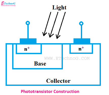
The construction of the phototransistor is almost the same as the normal transistor. It also three-layer and two junction devices. According to construction and layer, the phototransistor divided into two major types - 1. NPN 2. PNP
One of the major differences between the construction of a phototransistor and the normal transistor is phototransistor has a larger base and collector area than a normal transistor.
The base region of the phototransistor is exposed with a transparent material. So the light can easily enter and reach the base. Old phototransistors are designed and constructed with single semiconductor materials such as Silicon or Germanium but the modern phototransistors are constructed by gallium or arsenide to obtain higher efficiency.
When there is no light that falls upon the base of the phototransistor then also a low current flow due to the thermally generated electron-hole pairs. In absence of the light, the current flow through the phototransistor is known as dark current.
As the base and collector area of the phototransistor is larger so the base-collector junction is very sensitive to light. And its working very much depends upon the intensity of light. The increase in the level of light causes to increase in the flow of current.
Phototransistor Circuit Diagram
Here a circuit diagram of phototransistor with output load and Vcc power supply is given below.
You can see it is a light-operated relay using a phototransistor circuit. When light falls upon the phototransistor, it starts to conduct current, so current will flow through the phototransistor and also base to the emitter of the transistor T2. So the transistor T2 also starts to conduct the current and as it is connected to the relay, the relay will be turned on. Here the variable resistor is used to control the flow of current through the phototransistor as well as transistor T2. So the main function of this circuit is when the phototransistor detects light, the relay will be got turned on.
Phototransistor Connection Diagram
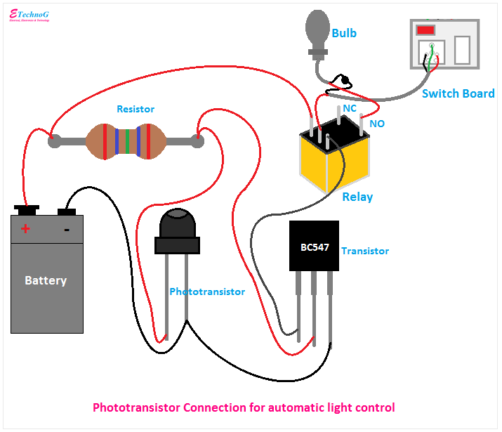
Here you can see the connection diagram of phototransistor for automatic light control during the darkness.
The main function of this connection is when the darkness will. occur, the light or bulb will automatically be turned on. Let's know how the circuit works. Its circuit is almost the same as the light control relay circuit using a phototransistor as we have seen in the before section. Just the difference is here the resistor is connected before the phototransistor. So when there is light available the phototransistor will conduct current means the current will flow through the resistor and the phototransistor, so no current will flow through the transistor T2(BC547).
When darkness occurs, the phototransistor will stop conducting current. So the current will flow through the resistor and the base to the emitter terminal of the transistor BC547. So the transistor will be turned on and it will cause to flow current through the relay coil. Once the relay coil got energized, it will make its NO contact with NC. So the light or bulb will be glow.
Read Also:


